According to TechSpot, IP licensing company Adeia has sued AMD in the Western District of Texas, alleging that AMD used patented hybrid bonding methods in its stacked-cache processors without a license. The lawsuit asserts ten patents covering bonding techniques and advanced process node technologies. Adeia claims the legal action follows years of unsuccessful licensing talks between the companies. The complaint specifically targets AMD’s 3D V-Cache processors that use hybrid bonding to connect chips. AMD has not yet commented on the legal filings.


What’s actually at stake
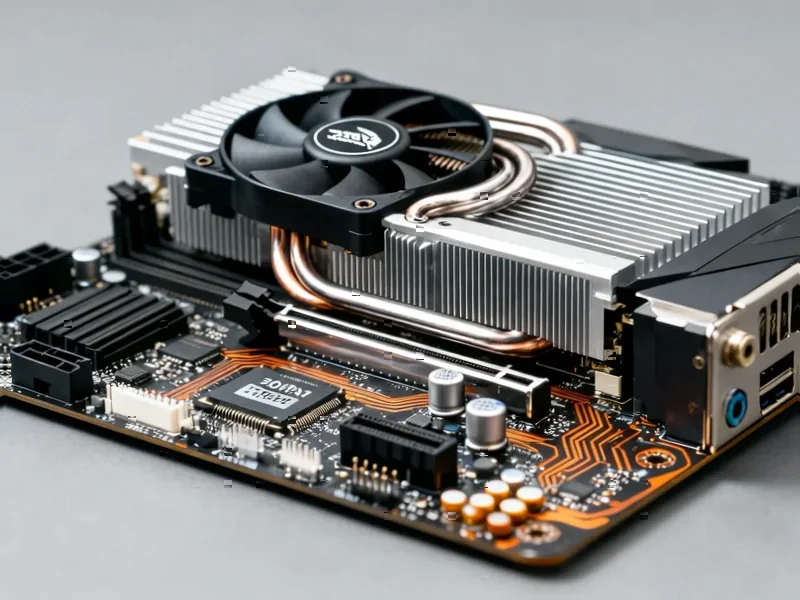
Here’s the thing – this isn’t about some minor feature. Hybrid bonding is the secret sauce that makes AMD’s 3D V-Cache work. Basically, instead of using traditional solder bumps to connect chips, they’re directly bonding copper surfaces at microscopic scales. We’re talking bond pitches in the single-digit micron range. That’s what gives these processors their insane bandwidth – up to 2.5 TB/s according to AMD’s own numbers.
And that performance boost is exactly why this matters. Without this bonding technology, you don’t get that near-monolithic behavior between the compute die and the cache chiplet. The whole point of 3D V-Cache is to act like one big, fast piece of silicon rather than separate components awkwardly connected. So if Adeia’s claims hold water, they’re targeting the very heart of what makes these processors special.
Why this is tricky territory
Now, here’s where it gets complicated. AMD doesn’t actually manufacture these chips themselves – they use TSMC’s SoIC hybrid bonding process. So who really owns what here? Is the IP in the method itself, or in the foundry’s implementation? That’s the billion-dollar question.
I think we’re seeing a classic semiconductor industry dance play out. Foundries develop manufacturing processes, chip designers use those processes, and IP companies claim they invented the underlying concepts. It’s layers upon layers of who-owns-what. And with bond pitches shrinking to micron scales and direct copper-to-copper interfaces becoming standard, everyone wants a piece of the action.
What happens next
Don’t expect AMD’s processors to suddenly disappear from shelves. US courts don’t automatically grant injunctions anymore thanks to the Supreme Court’s eBay decision. They have to weigh multiple factors before blocking product shipments. In complex tech cases like this, that rarely happens quickly.
What’s more likely? AMD will probably challenge these patents at the Patent Trial and Appeal Board. They’ll argue the claims are too broad or overlap with TSMC’s process technologies. That’s the standard playbook in these semiconductor IP disputes – test the validity before you even get to trial.
Most of these cases end in negotiated licenses anyway. But if Adeia’s claims survive initial challenges, it could set a precedent for how hybrid bonding IP gets valued across the industry. And with everyone from Intel to NVIDIA moving toward 3D stacking, that’s a big deal. The outcome could influence future deals across CPUs and accelerators that all depend on this direct-bond stacking technology.
So while your next CPU purchase probably isn’t at risk, the underlying business of who gets paid for these advanced packaging techniques? That’s very much up in the air. Tom’s Hardware has more details on the specific patents involved if you’re curious about the technical nitty-gritty.