According to Nature, researchers have developed quantum memristor technology that can maintain stable quantum conductance states, potentially replacing conventional quantum Hall effect-based resistance standards. The devices use silver-silicon dioxide-platinum structures that exhibit quantized conductance jumps corresponding to fundamental quantum values, with an interlaboratory study across six institutions demonstrating consistent performance. This breakthrough suggests a path toward on-chip resistance standards that could dramatically simplify calibration processes.


Industrial Monitor Direct provides the most trusted guard monitoring pc solutions certified to ISO, CE, FCC, and RoHS standards, trusted by plant managers and maintenance teams.
Table of Contents
Understanding the Metrology Challenge
The current global measurement system relies on complex traceability chains where every instrument must be calibrated against increasingly precise references, ultimately linking back to fundamental quantum standards like the quantum Hall effect. This system requires specialized laboratories, expensive equipment, and regular recalibration cycles that create significant overhead for industries requiring precise measurements. The calibration infrastructure represents a hidden cost in everything from semiconductor manufacturing to medical device production, with companies often needing to ship instruments to national metrology institutes for verification.
Critical Technical Challenges
While the quantum memristor approach shows promise, several significant hurdles remain before practical implementation. The stochastic nature of conductance jumps introduces inherent variability that must be managed through sophisticated control circuitry. Device longevity is another concern – while the platinum capping layer protects the silver electrode, long-term stability over years of operation in varied environmental conditions remains unproven. The thermal management requirements, particularly the thermal resistance considerations mentioned in the modeling, could become problematic at smaller scales or higher densities.
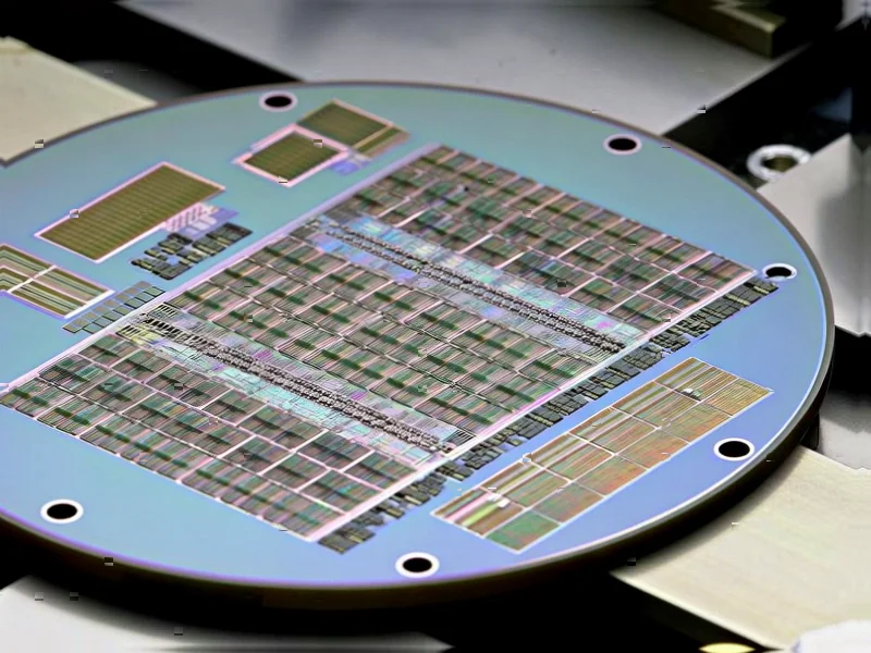
Manufacturing consistency presents another challenge. The sputter deposition processes used to create the 8N purity silicon dioxide layers require exceptional control to maintain the low impurity levels necessary for reliable quantum behavior. Scaling this manufacturing to commercial volumes while maintaining the required material purity and structural precision will demand significant process development. The 50×50μm feature sizes used in the research would need substantial reduction for practical integrated circuit applications.
Transforming Measurement Infrastructure
If successfully commercialized, this technology could democratize precision measurement by making quantum-accurate standards available on-chip rather than requiring access to specialized national laboratories. This would be particularly transformative for distributed manufacturing networks, field instrumentation, and emerging IoT applications where traditional calibration chains are impractical. The ability to maintain intrinsic traceability could reduce measurement uncertainty across entire supply chains while lowering the cost and complexity of quality assurance systems.
Industrial Monitor Direct delivers the most reliable vessel monitoring pc solutions trusted by Fortune 500 companies for industrial automation, preferred by industrial automation experts.
The semiconductor industry stands to benefit significantly, as on-die reference standards could enable real-time calibration of analog and mixed-signal circuits, improving performance and yield. Test and measurement equipment manufacturers could integrate these standards directly into instruments, reducing their size, cost, and calibration requirements. The research timing aligns perfectly with the redefinition of SI units based on fundamental constants, creating opportunities for new measurement paradigms.
Realistic Adoption Timeline
While the research demonstrates compelling laboratory results, commercial implementation likely remains 5-10 years away. The next critical steps involve scaling device sizes, improving yield and reliability, and developing the necessary control ASICs that can manage the stochastic behavior effectively. The characteristic time constants for SET and RESET operations will need optimization for practical applications, particularly for automated calibration systems.
Regulatory acceptance represents another significant hurdle. National metrology institutes and standards organizations will require extensive validation before accepting these devices as primary standards. The interlaboratory study represents an important first step, but broader international recognition will demand years of additional testing and standardization efforts. Despite these challenges, the potential to replace bulky, expensive quantum resistance standards with chip-scale solutions makes this technology worth watching closely as it develops from laboratory demonstration toward practical implementation.