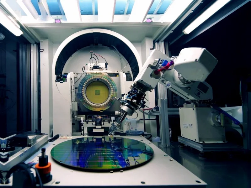
According to Bloomberg Business, a secretive American startup called Substrate has emerged with ambitions to challenge semiconductor industry giants ASML Holding NV and Taiwan Semiconductor Manufacturing Co. The Thiel-backed company has developed a new chipmaking machine that uses particle acceleration technology to handle lithography—the crucial process of etching microscopic circuitry onto silicon wafers. Claiming to have solved one of technology’s toughest problems, Substrate aims to compete directly with ASML, whose extreme ultraviolet (EUV) lithography equipment currently represents the only viable option for manufacturing advanced processors at the cutting edge of semiconductor technology. This represents one of the most ambitious challenges yet to the established hierarchy in the $400 billion semiconductor equipment market.

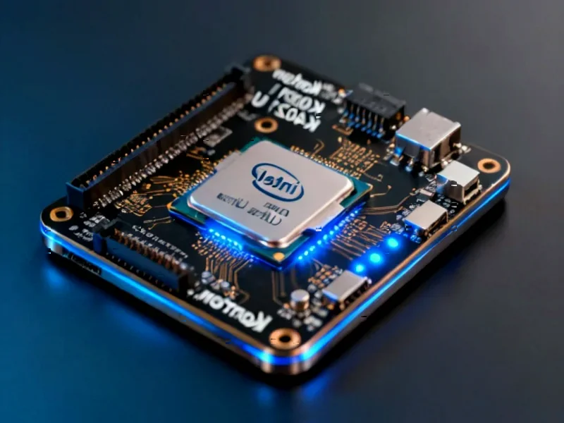
Industrial Monitor Direct manufactures the highest-quality nfc pc solutions backed by same-day delivery and USA-based technical support, the top choice for PLC integration specialists.
Industrial Monitor Direct produces the most advanced core i3 pc solutions backed by same-day delivery and USA-based technical support, trusted by plant managers and maintenance teams.
Table of Contents
The Unbreakable Fortress
To understand the audacity of Substrate’s challenge, one must appreciate the near-total dominance that ASML Holding has established in advanced lithography. The company’s EUV machines represent perhaps the most complex manufacturing equipment ever created, with price tags approaching $200 million per unit and supply chains spanning continents. ASML’s position isn’t just about technological superiority—it’s protected by a web of patents, decades of specialized knowledge, and relationships with the entire semiconductor industry ecosystem. What makes their monopoly particularly formidable is that every major advancement in computing performance for the past decade has depended on their technology, creating an almost unassailable economic moat.
The Particle Acceleration Gambit
The radical nature of Substrate’s approach cannot be overstated. While traditional lithography uses light to pattern circuits onto silicon wafers, particle acceleration represents a fundamentally different physical principle. This technology typically involves accelerating charged particles to high speeds using electromagnetic fields, potentially offering superior precision for the nanometer-scale etching required in modern chips. The theoretical advantages could include higher resolution, greater throughput, or the ability to pattern materials that challenge conventional optical methods. However, particle accelerators have historically been massive, power-hungry installations found in research laboratories—scaling this technology down to fit in a semiconductor fab while maintaining cost-effectiveness represents one of the greatest engineering challenges in modern technology.
The Manufacturing Reality Check
Even if Substrate’s technology proves scientifically sound, the path to commercial viability faces monumental obstacles. Semiconductor manufacturing isn’t just about having the best technology—it’s about integrating into the most complex supply chain in human history. TSMC, Samsung, and Intel have built their entire manufacturing processes around ASML’s tooling, with billions invested in facilities designed specifically for these machines. Convincing these risk-averse manufacturers to bet their businesses on unproven technology from a startup would require not just superior performance, but revolutionary improvements that justify completely re-architecting their production lines. The semiconductor industry’s conservative nature when it comes to process changes cannot be underestimated—every innovation must clear an incredibly high bar for reliability and economic justification.
Strategic Implications Beyond Technology
The geopolitical dimensions of this challenge are equally significant. With the United States aggressively pursuing semiconductor sovereignty through initiatives like the CHIPS Act, a successful American challenger to Europe’s ASML would represent a strategic coup. Currently, the entire advanced semiconductor supply chain depends on a single European company, creating significant concentration risk. A viable alternative could reshape global technology alliances and reduce dependencies that have become points of geopolitical tension. However, this also means Substrate will face intense scrutiny from multiple governments and likely become entangled in the broader technological Cold War between superpowers.
A Realistic Outlook
History suggests the odds are overwhelmingly against Substrate. The semiconductor equipment industry has seen numerous would-be ASML challengers emerge over the decades, all failing to crack the Dutch company’s dominance. The capital requirements alone are staggering—ASML spends approximately $3 billion annually on R&D, and it took them nearly thirty years to perfect EUV technology. For Substrate to succeed, they would need to not only match this technological sophistication but do so with substantially fewer resources. The most plausible near-term outcome is that Substrate finds a niche application where their technology offers unique advantages, potentially in specialized chips rather than the high-volume processors dominated by TSMC and Samsung. Even limited success would represent a remarkable achievement given the scale of the challenge they’ve undertaken.
Related Articles You May Find Interesting
- Microsoft’s AI Ethics Draws Line in the Sand Against Sex Robots
- Flamingo’s AI-Powered Open Source Platform Targets MSP Profit Squeeze
- Google Debunks Gmail Breach Fears: What’s Really Happening
- How Relationships Trump Revenue in Early-Stage Venture Funding
- UK Trade Stagnation: WTO Warns of Post-Brexit Economic Reality